


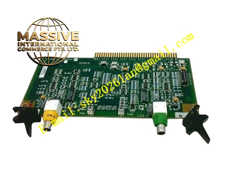
Description
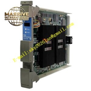
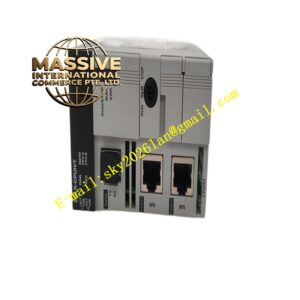
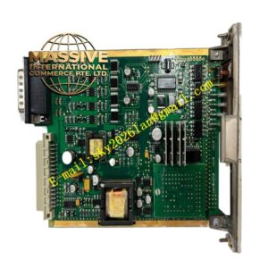
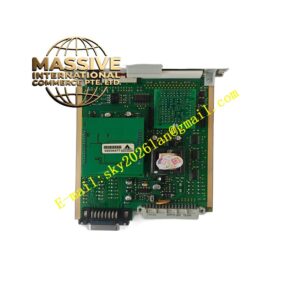
Honeywell 51305072-400
Technical Specifications
- Communication Bus: TDC3000 proprietary LCN bus, 5Mbps transmission rate
- Local I/O Bus: TDC3000 parallel I/O bus
- Power Supply: 5VDC and 12VDC from rack backplane
- Operating Ambient Temperature: 0°C to +60°C
- Storage Temperature: -40°C to +85°C
- Relative Humidity: 5% to 90% RH non-condensing
- Mounting Type: Plug-in slot installation on TDC3000 main control rack
- Certification: UL, CE, RoHS
- Maximum I/O Point Capacity: 512 points per interface board
Functional Features It receives LCN protocol frames from redundant LCN A and LCN B channels. It verifies frame checksum and filters invalid broadcast packets. It converts LCN network commands into local I/O bus instruction format. It executes cyclic polling scheduling for all connected local I/O modules. It collects analog input, digital input, analog output and digital output status data from I/O bus. It packages I/O data into standard LCN frames and sends to active LCN channel. It monitors LCN channel health and triggers automatic channel switchover when active link fails. It carries front panel LED indicators for power, LCN active, I/O bus active and fault. It supports hot swap replacement in redundant control node configuration. It records frame error count, bus timeout and I/O module offline logs and uploads diagnostic data to operator station.
Application Scenarios Large TDC3000 control node LCN to I/O bus gateway Petrochemical plant main control cabinet LCN I/O interface Refinery multi-loop control node communication board Power plant boiler integrated control rack LCN I/O adapter Chemical plant batch control system core network I/O bridge
Performance Parameters
- Redundant LCN Switchover Time: Less than 75ms
- Mean Time Between Failures: 740000 hours
- Insulation Resistance: Greater than 1000 MΩ
- ESD Immunity: 8kV contact discharge
- Maximum Frame Processing Rate: 15000 packets per second
Material Composition FR4 flame retardant conformal coated multilayer PCB 32-bit communication processing FPGA chip Dual LCN PHY transceiver chips Local I/O bus arbitration logic chip Non-volatile flash memory for configuration and log storage Isolation transformer and surge suppression TVS components Gold plated edge connector for TDC3000 backplane Metal front panel with extraction handle, LCN coaxial ports and LED indicators Internal aluminum heat sink for high-speed FPGA chip heat dissipation
Structural Features Standard TDC3000 paddle card form factor. Front panel integrates dual LCN coaxial signal ports, grouped LED indicators and extraction handle. Rear gold plated edge connector mates with rack backplane power, LCN signal and I/O bus signal. Internal PCB layout strictly separates high-speed LCN signal circuit and local I/O bus logic circuit to reduce crosstalk. Anti-key notch prevents reverse insertion into rack slot. Locking clip secures module firmly after installation. Independent shielding cavity for dual LCN channels isolates signal interference. Conformal coating covers PCB surface to resist moisture and corrosive gas in industrial cabinet.
Working Principle After receiving 5VDC and 12VDC power supply from rack backplane, the module completes power-on self-test and loads communication firmware from flash memory. It synchronizes clock signal with LCN bus and registers node address on LCN network. When LCN bus transmits command frames, transceiver chip receives analog signal and converts it into digital data. FPGA verifies frame validity and translates LCN command into local I/O bus signal. It sends polling command to I/O modules on local I/O bus and receives sampled I/O data. FPGA encapsulates I/O data into LCN frame and transmits to active LCN channel. If heartbeat packet loss is detected on active LCN channel, the module switches all communication traffic to standby LCN channel immediately. Fault and diagnostic data is uploaded to operator station.
Installation Requirements Wear anti-static wrist strap before inserting module into dedicated LCN I/O interface slot of rack. Lock extraction handle after full seating. Connect 75Ω LCN dedicated coaxial cable to LCN A and LCN B ports. Complete backplane wiring connection with local I/O bus expansion rack. Power on rack and wait for module self-test cycle to complete. Verify LCN A or LCN B active LED steady on. Configure node address and I/O point mapping in engineering workstation. Test redundant network switchover by disconnecting primary LCN cable. Confirm all I/O points keep normal communication during switchover test.
Usage Notes Only use 75Ω impedance matching LCN dedicated coaxial cable for network wiring. Do not scratch gold plated contact surface of edge connector. Keep cabinet ventilation channel unobstructed to avoid FPGA chip overheating. Do not remove conformal coating on PCB surface. Replace module when continuous communication timeout occurs and cable fault is excluded.