


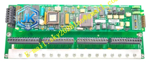
Description
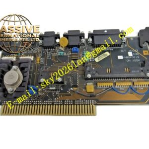
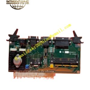
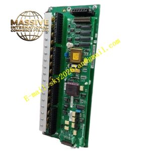
Honeywell 51309218-125
Technical Specifications Channel Count: 16 low-level analog input channels Input Signal Range: -50mV to +50mV Input Impedance: ≥100MΩ Excitation Output: Optional 0.5mA constant current per channel Power Supply: 5V DC Power Consumption: 6.9W Operating Temperature Range: 0℃ to 60℃ Storage Temperature Range: -40℃ to 85℃ Isolation Withstand Voltage: 1500V AC Relative Humidity: 5% to 95%, non-condensing
Functional Features It integrates programmable gain amplifier for each channel to adapt different low-level signal amplitude. It carries out multi-stage hardware low-pass filtering to suppress industrial high-frequency noise. It detects open circuit of field sensor wiring and uploads fault alarm. It supports hot swap operation. It stores gain configuration and channel calibration parameters in non-volatile memory. It executes channel zero offset compensation automatically. It uploads raw sampling value and channel diagnostic status to the DCS system.
Application Scenarios Strain gauge force and weight measurement for material testing and weighing systems. Tiny pressure signal acquisition from low-output differential pressure sensors. Small displacement sensor signal collection for mechanical equipment monitoring. Replacement and spare stocking for aging low-level analog multiplexer cards in legacy TPS systems.
Performance Parameters Measurement Resolution: 0.1μV Full Scale Accuracy: ±0.15% FS Channel Scan Period: 2ms per channel Gain Adjustment Range: 1 times to 1000 times Non-volatile memory retention time: 10 years without external power supply
Material Composition PCB Substrate: High-TG flame-retardant FR-4 multi-layer glass fiber board, strict analog-digital zoning layout High-precision programmable instrumentation amplifier chip Multi-order LC filter network components High-resolution ADC conversion chip Gold-plated back edge fingers Gold-plated field terminal block contacts Cold-rolled steel front panel with electrostatic spray coating
Structural Features Standard European pluggable card structure, installed in dedicated low-level analog I/O slot of UCN I/O rack. Front panel is equipped with run indicator light, fault indicator light and channel fault indicator light. Field wiring terminals are arranged on the side panel for low-level sensor cable connection. All weak signal traces adopt double-layer shielding layout to isolate external electromagnetic interference. Amplifier chips are equipped with independent heat isolation structure to reduce thermal drift.
Working Principle Weak millivolt or microvolt signals from field sensors enter the module through shielded cables. The programmable gain amplifier amplifies the signal to suitable acquisition range according to channel configuration. The multi-stage filter circuit removes high-frequency noise superimposed on the signal. The high-resolution ADC converts conditioned analog signal into digital value. The FPGA chip executes zero offset compensation and gain correction, and transmits sampling data and fault status to the rack IOP processor through backplane bus. It records open-circuit and over-range fault events with time stamp.
Installation Requirements Insert the module vertically into the dedicated analog I/O slot of UCN rack and tighten front panel fixing screws. Connect shielded twisted pair sensor cables to the corresponding terminal ports. Ground the shielding layer of field cables at the module side only, avoid double-point grounding. Download channel gain and filter configuration parameters from Control Builder software after power on. Verify sampling value stability and zero fault alarm on the HPM diagnostic screen.
Precautions Release static electricity before plugging the module to protect high-sensitivity analog amplifier circuit. Low-level signal cables must be separated from high-power AC cables to avoid induction noise. Double-point grounding of shielding layer will introduce ground loop and cause signal drift. Do not apply voltage signal exceeding ±50mV to the input channel, which will damage the amplifier circuit. This module is not suitable for standard 4-20mA transmitter signal acquisition.