


Description
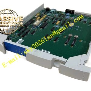
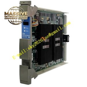
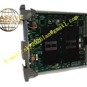
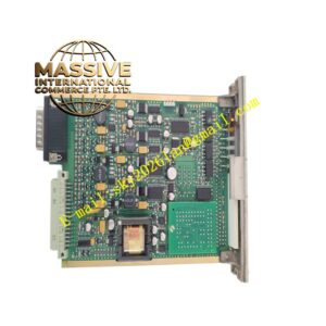
Honeywell 51200641-101
Technical Specifications LCN Bus Rate: 5Mbps Backplane Interface: Parallel local node backplane bus Logic Power Supply: 5V DC Power Consumption: 7.2W Operating Temperature Range: 0℃ to 65℃ Storage Temperature Range: -40℃ to 85℃ Isolation Withstand Voltage: 1500V AC Relative Humidity: 5% to 95%, non-condensing On-board Buffer Capacity: 128KB
Functional Features It provides bidirectional data frame buffering for LCN bus and local node processor. It executes frame sorting, priority classification and retransmission scheduling for alarm and command frames. It implements CRC check for all buffered data frames. It supports bus congestion control and frame flow limiting. It stores communication statistical data and fault log in non-volatile memory. It uploads buffer overflow and communication timeout alarm to LCN network diagnostic console. It distributes unified system time synchronization frame to local node processor.
Application Scenarios Communication adaptation for GUS operator stations and HM history modules. Data forwarding buffer for NIM gateway modules connecting LCN and UCN subnets. Replacement and spare stocking for aging LCN communication adapter boards of legacy TPS cabinets. Bus load optimization for multi-node LCN network in large petrochemical control systems.
Performance Parameters Frame Forwarding Latency: ≤80μs Buffer Overflow Detection Threshold: 90% of total buffer capacity Frame Error Log Storage Capacity: 3000 communication fault records Maximum Supported Concurrent Frame Quantity: 120 frames
Material Composition PCB Substrate: High-TG FR-4 multi-layer board with signal isolation layout FPGA frame processing and control chip High-speed SRAM buffer memory chips Bus transceiver and level conversion chips Gold-plated back edge fingers Cold-rolled steel front panel with electrostatic spray coating
Structural Features Standard European pluggable card structure, installed in dedicated LCN adapter slot of LCN node rack. Front panel is equipped with run indicator light, buffer overflow indicator light and fault indicator light. Back edge gold fingers realize electrical connection with node backplane bus. High-speed signal traces adopt shielding layout to reduce crosstalk. Buffer memory chips are arranged close to FPGA chip to shorten signal transmission path.
Working Principle After power-on initialization, the board establishes handshake connection with local node processor and LCN bus interface board. Data frames from local processor enter the on-board buffer, the FPGA chip classifies frame priority and sends frames to LCN bus interface board in sequence. Incoming frames from LCN bus enter the buffer, the chip completes frame verification and forwards valid frames to local node processor. When buffer occupancy exceeds threshold, the board triggers overflow alarm and discards low priority frames temporarily. It records communication fault events and uploads alarm information to LCN diagnostic console.
Installation Requirements Insert the board vertically into the dedicated LCN adapter slot of LCN node rack and tighten fixing screws. Confirm backplane pin alignment before full insertion. Download communication priority and buffer threshold parameters from LCN configuration software after power-on. Verify frame forwarding status and buffer occupancy on the LCN network diagnostic page.
Precautions Release static electricity before plugging the board to protect FPGA and memory chips. Do not apply voltage beyond 5V DC specification to the backplane interface. Buffer overflow leads to temporary loss of low priority trend data. This board must work with matched LCN bus interface board and node processor, it cannot operate independently. High ambient temperature accelerates aging of buffer memory chips and causes data read error.