


Description
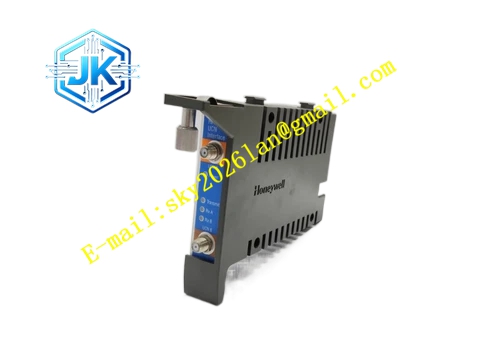
Honeywell 51402573-150
Technical Specifications Data Bus Width: 32-bit parallel data bus Address Bus: 24-bit address bus Maximum Supported Memory Capacity: 128MB Data Access Clock: 33MHz Power Supply: 5V DC Power Consumption: 6.2W Operating Temperature Range: 0℃ to 65℃ Storage Temperature Range: -40℃ to 85℃ Isolation Withstand Voltage: 1500V AC Relative Humidity: 5% to 95%, non-condensing
Functional Features It executes address decoding, read/write timing control and data latch for memory access operation. It integrates ECC error checking and correction function for single-bit memory error. It carries out memory chip offline detection and bad block marking during node startup. It supports hot swap operation in redundant LCN node configuration. It stores memory mapping table and fault log data in non-volatile memory. It uploads memory access error, parity error and chip failure alarm to the LCN network diagnostic console. It supports burst data transmission for continuous trend recording.
Application Scenarios Memory interface control for HM history module racks storing process trend and alarm records. High-speed memory access support for GUS operator station and engineering station LCN nodes. Replacement and upgrade of old revision memory interface modules in legacy TPS LCN cabinets. Stable data storage service for LCN nodes with heavy historical data recording load.
Performance Parameters Single Read Access Latency: ≤30ns ECC Correction Speed: ≤12ns per error bit Memory Chip Fault Detection Time: 200ms during startup self-test Fault Log Storage Capacity: 150 memory error historical records
Material Composition PCB Substrate: High-TG FR-4 multi-layer board with controlled impedance bus layout Bus interface logic FPGA chip ECC error correction processing chip Signal buffer and driving components Gold-plated back edge fingers Gold-plated memory bank connector contacts Cold-rolled steel front panel with electrostatic spray coating
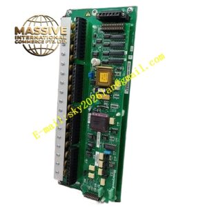
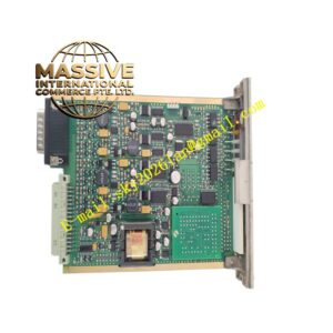
Structural Features Standard European pluggable card structure, installed in dedicated memory interface slot of LCN node rack. Front panel is equipped with run indicator light, data access indicator light and memory fault indicator light. High-density memory bank connector is arranged on the side panel for memory chip array connection. Address bus and data bus traces adopt equal-length routing to guarantee synchronous signal timing. Logic circuit and memory bus circuit are separated by isolation barrier.
Working Principle The module receives address, read/write command and control signal from LCN node main processor through backplane bus. The address decoding logic selects the target memory chip and memory address. The timing control circuit generates stable read or write strobe signal. During read operation, the module receives data from memory bank, executes ECC check and correction, then transmits corrected data back to main processor. During write operation, the module adds ECC check code to data stream and writes data into target memory address. When memory access error or chip failure is detected, the module triggers local LED alarm and uploads fault event to LCN diagnostic system.
Installation Requirements Insert the module vertically into the dedicated memory interface slot of LCN node rack and tighten fixing screws. Connect memory bank flat ribbon cable to the side panel connector, confirm cable direction matches marking. Download memory mapping configuration parameters from LCN node configuration software after power on. Run memory self-test program and verify error correction function on the LCN diagnostic page.
Precautions Release static electricity before plugging the module to protect high-speed bus logic chips. Do not remove memory ribbon cable when the node rack is powered on. Dust accumulation on memory connector pins causes intermittent data reading error. Memory chip combination must match the mapping table configured in this module. This module cannot work independently without matched memory bank assembly.