


Description
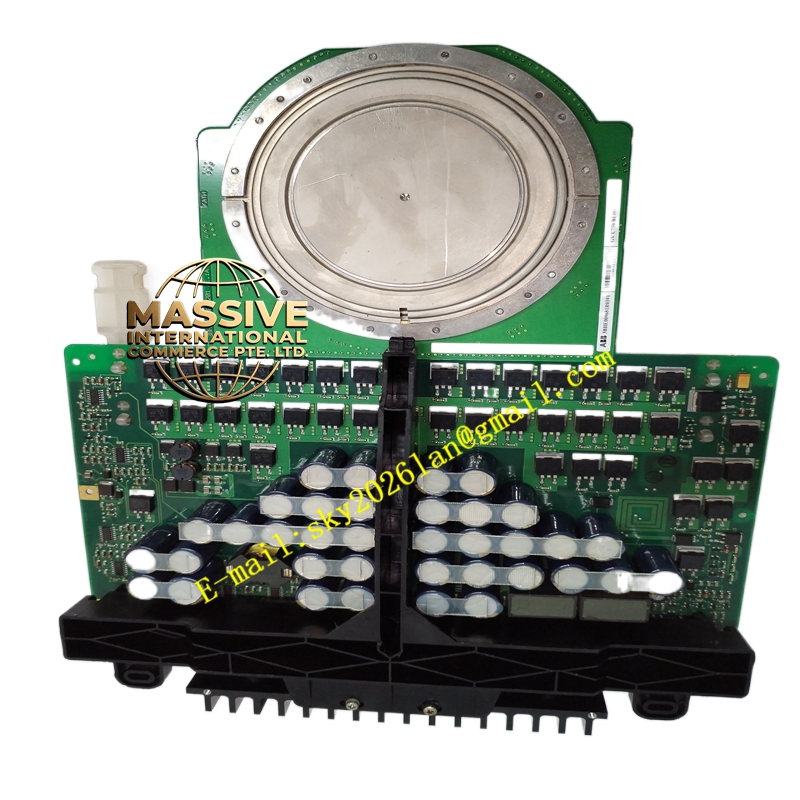
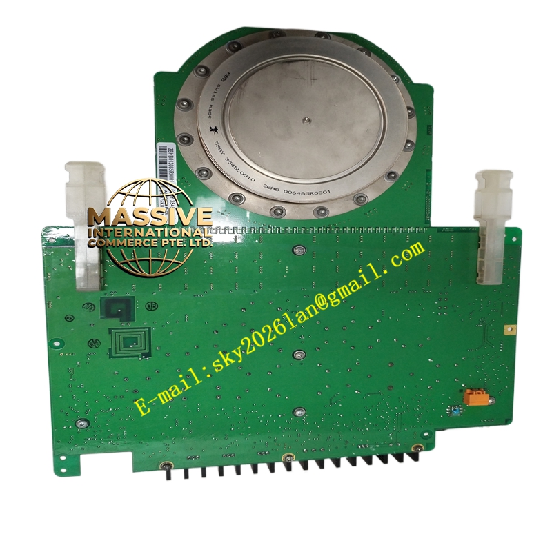
ABB 5SHY3545L0009
Technical Specifications:
- Device Type: Asymmetric IGCT (Non-symmetrical structure with lower leakage current).
- Voltage Rating: 6 kV (High blocking voltage).
- Current Rating: 4500 A (High conduction current density).
- Power Capacity: 27 MW.
- Switching Frequency: Up to 2 kHz.
- Efficiency: Greater than 98%.
- Protection Rating: IP67.
- Operating Temperature Range: -40°C to +85°C.
- Dimensions: 439 mm (Length) x 173 mm (Width) x 41 mm (Height).
- Weight: 2.9 kg.
Functional Features:
- Superior Switching Performance: Features excellent turn-off performance and low switching losses, allowing for high-frequency operation without bulky snubber circuits.
- Low Conduction Losses: Exceptionally low on-state voltage drop ensures high efficiency and minimal heat generation during continuous operation.
- High Reliability: The asymmetric structure provides superior thermal stability, high dielectric strength, and excellent resistance to voltage surges.
- Integrated Drive: Combines the GTO chip, anti-parallel diode, and gate drive circuit into a single low-inductance package.
Application Scenarios:
- Medium-voltage AC and DC motor drives (e.g., ABB ACS series inverters).
- High-Voltage Direct Current (HVDC) transmission systems and Flexible AC Transmission Systems (FACTS).
- Renewable energy generation, including wind turbine converters and hydroelectric systems.
- Modular Multilevel Converters (MMC) for railway traction power supplies.
Material Composition & Structural Characteristics:
- Semiconductor Die: Silicon-based asymmetric IGCT wafer utilizing non-symmetrical doping technology.
- Packaging: Press-pack housing constructed from high-strength, electrically insulated materials.
- Terminals: High-conductivity copper contacts optimized for low-inductance busbar connections.
- Thermal Interface: Designed for direct press-fit mounting against high-performance heat sinks.
Working Principle:
In the on-state, the IGCT acts as a positive feedback switch (similar to a thyristor), carrying high current with a very low voltage drop. To turn off the device, the integrated gate drive forces the entire anode current to transfer to the gate circuit within microseconds. This rapidly reverse-biases the cathode junction, turning the device into a transistor-like mode and completely blocking the current. This zero-voltage switching mechanism eliminates the need for external protective snubber circuits.
Installation Requirements:
- Press-Fit Force: Must be installed using a precision press-fit mechanism with a uniform clamping force across the entire surface area to ensure optimal thermal and electrical contact.
- Heat Sink Interface: Requires a highly polished, flat heat sink surface with appropriate thermal interface material (grease or pads).
- Busbar Design: The DC link busbars must be designed with extremely low stray inductance to prevent voltage spikes during high-speed switching.
- Alignment: Ensure perfect mechanical alignment to prevent cracking of the semiconductor wafer during clamping.
Usage Precautions:
- Clamping Force: Strictly adhere to the manufacturer’s specified clamping force; insufficient force causes thermal runaway, while excessive force cracks the silicon.
- Gate Drive Power: Ensure the dedicated gate drive unit provides the precise peak current and di/dt required for reliable turn-off.
- Electrostatic Discharge (ESD): Handle with ESD-safe equipment to prevent damage to the sensitive gate structure.
- Cooling System: Verify that the cooling system is fully operational before applying high voltage or current to prevent immediate thermal destruction.