


Description
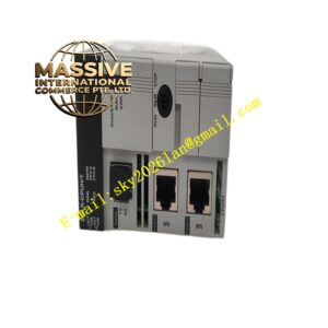
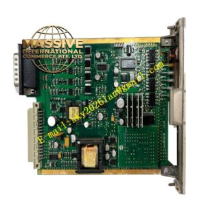
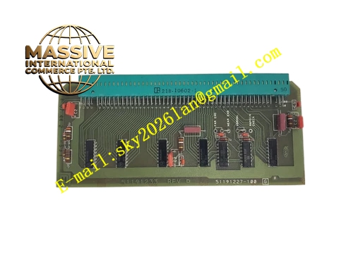
Honeywell 51196653-100
Technical Specifications
- Memory Type: High speed asynchronous SRAM
- Total Memory Capacity: Fixed onboard memory density
- Data Bus Width: 32bit data bus matching controller CPU
- Access Time: 85ns maximum access cycle
- Supply Voltage: 5V DC from controller motherboard
- Operating Temperature: 0°C to +60°C
- Interface: Board-to-board memory socket connector
- Parity Check: Byte wise parity generation and checking
Functional Features Parity error detection for every memory read and write operation. Memory space mapped to controller address bus automatically after power on. Expansion memory and onboard base memory operate as contiguous address space. No software configuration required for memory mapping. Low power consumption design, no extra cooling requirement for controller chassis. Parity fault signal sent to controller fault register for alarm reporting.
Application Scenarios DCS controller memory chip failure replacement Controller configuration expansion requiring larger runtime memory Trend recording buffer capacity upgrade Legacy process control system overhaul spare parts
Performance Parameters
- Parity error detection coverage: 100% per byte
- Data retention: Volatile, all data cleared after power loss
- Bus loading: Controlled bus capacitance to avoid timing violation
- Parity fault response: Immediate fault flag assertion upon parity mismatch
Material Composition High speed FR4 PCB, SRAM memory ICs, parity logic gate array, decoupling ceramic capacitors, pull-up metal film resistors, gold plated board-to-board memory connector, ESD protection diodes.
Structural Features Small vertical plug-in daughter board. Single edge gold connector for mating with CPU motherboard memory socket. No external wiring terminals. Component layout optimized for signal length matching to maintain bus timing. Silk screen marking for orientation identification.
Working Principle After controller power up, memory controller performs automatic memory scan and identifies this expansion board. Memory space is merged into main address map. CPU writes control program runtime variables, trend samples and alarm event records into SRAM chips. Each write cycle generates parity bit and stores together with data. Read operation recalculates parity and compares stored parity value. Mismatch triggers parity fault alarm. All data is lost once controller power supply is removed.
Installation Requirements Power down controller completely and discharge residual voltage before installation. Align board orientation marker and insert vertically into memory socket until fully seated. Restart controller and enter system diagnostic screen to verify total recognized memory size. Ensure controller internal cooling airflow passes over memory board surface.
Usage Notes Static electricity will destroy memory chips, anti-static handling is mandatory. This memory board does not provide non-volatile storage, control strategy is stored in separate flash or EPROM device. Parity error indicates memory hardware fault, replace board immediately. Do not bend connector pins during insertion and removal.