


Description
KLA-Tencor 2114B-30SLT
Technical Specifications High resolution optical sensing assembly; precision linear positioning stage interface; low vibration mechanical structure; cleanroom low outgassing material construction; high speed digital signal output; controlled operating temperature range for semiconductor fab environments.
Functional Features Captures high magnification optical images of patterned and bare silicon wafers. Identifies microscale surface defects, particles and lithography pattern deviations. Transmits image and defect coordinate data to the host inspection tool processor. Supports synchronized scanning motion with the wafer positioning stage. Includes internal diagnostic monitoring for optical and motion subsystem health.
Application Scenarios Semiconductor wafer fabrication cleanrooms, integrated circuit lithography process control, post etch and post deposition defect inspection.
Performance Parameters Submicron defect detection resolution; low image noise; stable optical alignment under cleanroom thermal conditions; high scanning throughput compatible with production wafer lots.
Material Composition Structural frame uses low thermal expansion alloy; optical lens components use precision optical glass with anti‑reflection coating; mechanical moving parts use hardened corrosion resistant alloy; electronic circuit substrates are low particle FR‑4 PCB; sealing materials are low outgassing fluoropolymer.
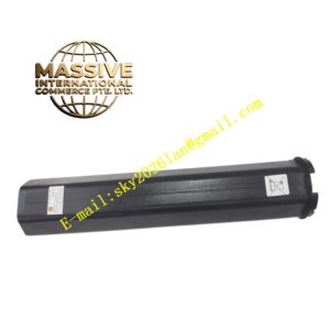
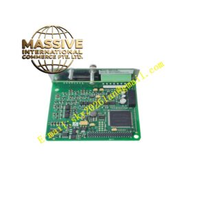
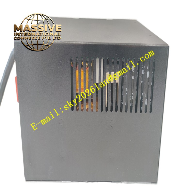
Structural Characteristics Integrated optical head assembly mounted on precision scanning stage; internal optical path enclosed within light shielding housing; flex cable and high speed data connectors for image transmission; precision alignment adjustment screws for optical calibration.
Working Principle Illumination light passes through the optical lens assembly and projects onto the wafer surface. Reflected and scattered light is collected by optical sensors and converted into digital image data. The host system analyzes pixel data to locate defects and record defect coordinates while the stage moves the wafer under the optical head in controlled scanning motion.
Installation Requirements Perform all handling in class rated cleanroom conditions with anti-static wrist straps and gloves. Align the optical assembly to the tool base with precision fixture tooling. Lock out main equipment power before mechanical installation. Complete optical focus and offset calibration after mounting.
Precautions for Use Optical surfaces must not be touched by bare hands. Prevent exposure to process vapors, photoresist aerosols and particulate contamination. Operate only within the original matched KLA-Tencor inspection tool platform.