


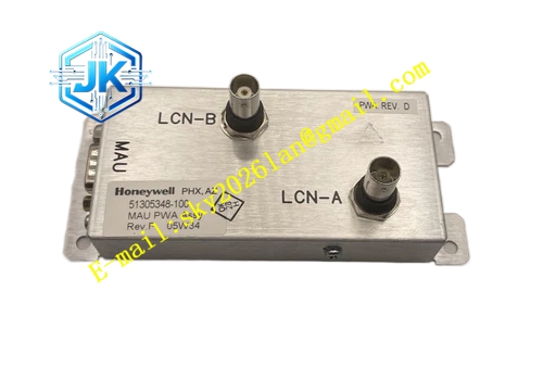
Description
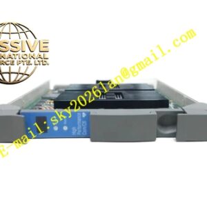
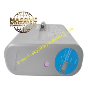
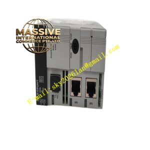
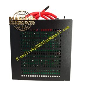
Honeywell 51305348-100
Technical Specifications Channel Count: 8 analog output channels Output Signal Range: 4mA to 20mA DC Maximum Output Load Resistance: 750Ω per channel Logic Power Supply: 5V DC Power Consumption: 6.8W Operating Temperature Range: 0℃ to 60℃ Storage Temperature Range: -40℃ to 85℃ Isolation Withstand Voltage: 1500V AC per channel group Relative Humidity: 5% to 95%, non-condensing
Functional Features It provides group-based galvanic isolation for analog output channels. It supports configurable output range and fail-safe state for each channel. It executes output circuit fault detection including open circuit and over-load alarm. It supports hot swap operation within powered UCN I/O rack. It stores channel scaling, fail-safe value and output filtering parameters in non-volatile memory. It uploads real-time output value and channel fault status to DCS system. It supports configurable low-pass digital filter to smooth output signal jitter.
Application Scenarios Control output for regulating valves of temperature, pressure, flow and liquid level control loops. Drive signal output for I/P converters and pneumatic valve positioners. Analog output for variable frequency speed regulation auxiliary control signals. Replacement and spare stocking for aging analog output cards in legacy TPS UCN racks.
Performance Parameters DAC Resolution: 16 bit Full Scale Accuracy: ±0.1% FS Channel Update Cycle: 2ms per channel Over-load Detection Threshold: 800Ω load resistance Open circuit detection threshold: <3.2mA output current
Material Composition PCB Substrate: High-TG flame-retardant FR-4 multi-layer glass fiber board, analog and digital circuit partition layout High-precision DAC digital-to-analog conversion chip Signal conditioning and current driving components Channel group isolation optocoupler chips Gold-plated back edge fingers Gold-plated ribbon cable connector contacts Cold-rolled steel front panel with electrostatic spray coating
Structural Features Standard European pluggable card structure, installed in dedicated analog output slot of UCN I/O rack. Front panel is equipped with RUN indicator light, group fault indicator lights and general fault indicator light. Ribbon cable connector is arranged on the side panel for connection to matched analog output FTA termination assemblies. Analog signal traces are surrounded by shielding copper layer to reduce crosstalk and electromagnetic interference. Each group of 4 channels adopts independent isolation barrier to prevent fault cross transmission between channels.
Working Principle Digital control commands from HPM main processor transmit to the card through backplane bus. The FPGA chip receives digital setpoint data and sends data to DAC conversion chip. The DAC chip converts digital value into analog voltage signal. The driving circuit converts voltage signal into stable 4-20mA current signal. The conditioned analog signal transmits to matched analog output FTA assembly via ribbon cable and then to field valve actuator. The supervision circuit continuously monitors output loop current and load impedance. When open circuit or over-load fault occurs, the card marks corresponding channel fault and uploads alarm to DCS system.
Installation Requirements Insert the card vertically into the dedicated analog output slot of UCN rack and tighten front panel fixing screws. Connect the card with matched analog output FTA termination assembly using factory specified ribbon cable. Confirm ribbon cable pin definition and insertion direction before power supply switch-on. Download channel scaling, fail-safe value and filter parameters from Control Builder software after power-on. Verify output accuracy and fault alarm function on HPM diagnostic screen.
Precautions Release static electricity before plugging the card to protect high-precision DAC circuit. Do not connect high voltage AC signals to matched FTA output terminals. Analog output wiring must be separated from high-power inverter and AC power cables. Loose ribbon cable connection causes output signal jumping and intermittent control failure. Confirm field valve load resistance matches module specification before commissioning.