


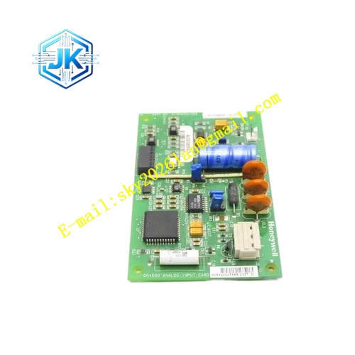
Description
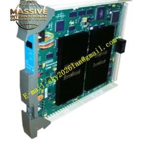
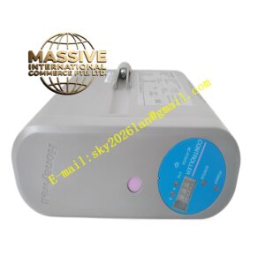
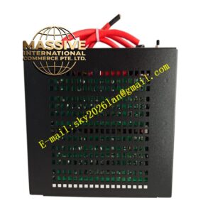
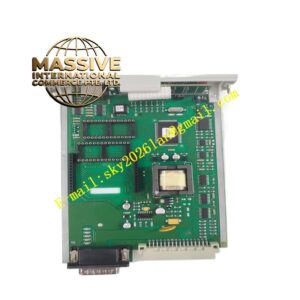
Honeywell 51200844-100
Technical Specifications LCN Bus Rate: 5Mbps Bus Medium: 50Ω coaxial cable Logic Power Supply: 5V DC Power Consumption: 5.3W Operating Temperature Range: 0℃ to 65℃ Storage Temperature Range: -40℃ to 85℃ Isolation Withstand Voltage: 1500V AC Relative Humidity: 5% to 95%, non-condensing On-board Buffer Capacity: 64KB
Functional Features It shapes distorted bus signal waveform and suppresses high-frequency electromagnetic noise. It provides bidirectional data frame buffer for LCN bus interface and node processor. It assists bus arbitration logic to reduce frame conflict probability on shared LCN bus. It counts frame error, signal attenuation and bus timeout events. It stores network fault statistics and alarm logs in non-volatile memory. It supports redundant A/B bus signal switching coordination. It uploads network diagnostic data to LCN network management console.
Application Scenarios Auxiliary signal processing for GUS operator station LCN communication nodes. Network signal stabilization for HM history module and NIM gateway nodes. Replacement and spare stocking for aging LCN auxiliary boards of legacy TPS control cabinets. Signal conditioning for LCN nodes installed in high electromagnetic interference workshop areas.
Performance Parameters Signal Shaping Delay: ≤45μs Frame Error Log Storage Capacity: 2000 network fault records Signal Attenuation Monitoring Resolution: 0.02dB Buffer Overflow Detection Threshold: 90% of total buffer capacity
Material Composition PCB Substrate: Low-loss controlled impedance FR-4 multi-layer board Signal conditioning and buffer FPGA chip High-speed SRAM memory chips RF matching and transient suppression components Gold-plated back edge fingers Cold-rolled steel front panel with electrostatic spray coating Metal shielding cover for high-frequency signal area
Structural Features Standard pluggable board structure, installed in dedicated auxiliary slot of LCN node rack. Front panel is equipped with RUN, A-BUS FAULT, B-BUS FAULT and BUFFER OVERFLOW indicator lights. Back edge gold fingers connect with node backplane bus. High-frequency RF signal area adopts independent metal shielding cover to isolate digital logic noise. Signal traces adopt controlled impedance routing to match 50Ω LCN bus characteristic impedance.
Working Principle After power-on initialization, the board establishes handshake connection with LCN bus interface board and node processor. Incoming analog RF signals from LCN coaxial bus enter the board, the conditioning circuit reshapes distorted waveform and filters interference noise. Valid data frames enter on-board buffer and transmit to local node processor. Outgoing frames from node processor enter buffer, the board completes priority sorting and sends frames to LCN bus interface board. It continuously monitors bus signal quality and frame error rate. When signal quality exceeds threshold, it generates fault alarm and records fault timestamp.
Installation Requirements Insert the board vertically into the dedicated LCN auxiliary slot of node rack and tighten fixing screws. Confirm backplane pin definition and insertion direction before power supply switch-on. Download network diagnostic threshold parameters through LCN configuration software after power-on. Check bus signal quality and fault statistical data on LCN network diagnostic page.
Precautions Release static electricity before plugging the board to protect FPGA and RF signal chips. Do not use non-50Ω coaxial cables for LCN bus wiring. Metal dust accumulation on the shielding cover degrades signal anti-interference performance. This board must work together with matched LCN bus interface board, it cannot work independently. Excessive bus load causes frequent buffer overflow and frame loss.