


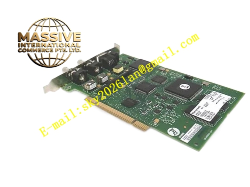
Description
Honeywell TC-PCIC02
Technical Specifications
- Compatible device: C200 redundant controller
- Bus interface: Dual redundant PCIe expansion bus
- Communication rate: 1 Gbps
- Maximum connected I/O substations per card: 4
- Supply power: 5 V DC drawn from controller backplane
- Operating temperature: 0 °C to +60 °C
- Isolation withstand voltage: 1500 VAC for 1 minute
- Hot swap support: Online replacement for faulty communication cards
Functional Features Dual redundant communication links, seamless switchover to backup link when the primary link fails. On-board signal shaping circuit compensates for signal attenuation over long-distance bus runs. CRC communication verification for all data frames, transmission bit error rate below 10^-12. Real-time link fault diagnosis, triggers controller redundancy communication alarm. On-board LEDs indicate Link A, Link B communication status and fault status. Supports online firmware upgrade, no card disassembly required for logic updates.
Application Scenarios Redundant communication link assembly for C200 controllers Spare part replacement for data packet loss and link faults in legacy communication cards Communication connection for C200 system I/O substation expansion Communication unit assembly for high-availability control systems
Performance Parameters
- Link switchover time: ≤1 ms
- Communication latency: ≤100 μs
- Maximum bus transmission distance: 10 meters shielded twisted pair
- Fault detection response: ≤50 ms
- Mean time between failures: 500,000 hours
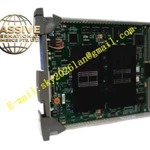
Material Composition FR4 high-speed PCB substrate PCIe bus transceiver chip FPGA communication logic chip High-speed optocoupler isolation array Gold-plated backplane edge fingers Metal shielded front panel
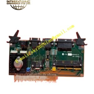
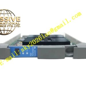
Structural Features Standard Eurocard dimensions, inserts into the dedicated communication slot of the C200 controller. Front panel features two redundant bus interfaces for connecting expansion I/O subracks. LED array indicates A and B link status. Metal shielded enclosure isolates high-speed bus electromagnetic radiation. Equal-length differential traces maintain consistent signal delay across dual links.
Working Principle After insertion into the controller backplane, the FPGA initializes PCIe communication logic, establishing a data channel with the main processor. Controller-issued I/O commands travel over the dual redundant links to field I/O substations; field-acquired data returns over the links to the card, packaged for transmission to the controller for logic computation. Link monitoring circuit continuously checks signal integrity on both communication paths; when the active link is abnormal, automatic switchover to the backup link occurs. CRC verification circuit checks every transmitted frame, automatically triggering retransmission for corrupted data.
Installation Requirements Insert the card into the dedicated slot only when rack power is off, press evenly until gold fingers are fully seated. Connect dual redundant bus flat cables to A and B channels, lock the connector clips to prevent loosening. Check LED status after power-up, confirm both links show normal communication lock. Wear an anti-static wrist strap when handling the card to avoid ESD damage to the FPGA.
Usage Notes Hot-swapping the communication card causes all connected I/O substations to drop offline, triggering process alarms. Oxidized connector contacts cause communication packet loss; clean gold contacts regularly. Dual-link card firmware version must match the main controller firmware; mismatched versions prevent card recognition. Never bend expansion flat cables to radius smaller than 5 cm, this breaks internal conductors.