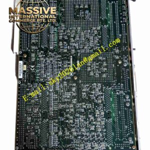




Description
Motorola MVME187-004A
Technical Specifications
- Processor: Features a 32-bit MC88100 Microprocessor Unit (MPU) paired with two MC88200 or MC88204 Cache/Memory Management Units (CMMUs) for high-speed data processing and virtual memory management.
- Memory: Supports scalable onboard DRAM, offering 4/8/16/32/64 MB with parity protection, or up to 128/256 MB with ECC (Error-Correcting Code) protection.
- Storage: Equipped with four 44-pin PLCC ROM sockets (organized in two 32-bit banks) and 128 KB of Static RAM (SRAM).
- Non-Volatile Memory: Includes 8 KB of battery-backed SRAM and a real-time clock to preserve critical system configurations and time-of-day data during power loss.
Functional Features
- Advanced Debugging: Comes pre-loaded with 187Bug debug monitor firmware, providing over 50 debug commands, disk bootstrap loading, up/down load capabilities, and a one-line assembler/disassembler.
- High-Speed Networking: Integrates an 82596CA Ethernet controller that utilizes Direct Memory Access (DMA) to access local RAM efficiently, with each board featuring a globally unique MAC address.
- Comprehensive I/O: Provides multiple EIA-232-D serial ports, a Centronics parallel printer port, and a full SCSI bus interface for connecting high-speed storage peripherals.
- System Control: Can be configured via a jumper on header J2 to act as the VMEbus system controller, managing bus arbitration and interrupt handling.
Application Scenarios
Widely deployed in aerospace test equipment, defense radar and sonar systems, telecommunications switching infrastructure, semiconductor manufacturing, and large-scale Distributed Control Systems (DCS).
Performance Parameters
- Bus Architecture: Operates as a 32-bit address and 32-bit data (A32/D32) VMEbus master/slave, while also supporting legacy A16/A24 and D8/D16 devices.
- Timer Resources: Includes four 32-bit programmable tick timers with 1 µs resolution, a hardware watchdog timer, and software-programmable hardware interrupts.
- Memory Access: The onboard DRAM is four-way interleaved to efficiently support cache burst cycles, maximizing the RISC processor’s throughput.
Material Composition
Constructed using multi-layer, industrial-grade printed circuit boards (PCBs) with high-Tg (glass transition temperature) materials. Core components are rigorously screened for high reliability, and the board is designed to withstand harsh industrial environments.
Structural Characteristics
Conforms to the standard 6U double-height VME form factor. The front panel features a comprehensive array of status indicator LEDs (including Power, Fail, Stat, Run, SCON, and SCSI) and physical switches for system reset and abort functions.
Working Principle
Upon system power-up, the MC88100 MPU executes initialization code from the onboard EPROMs. The 187Bug firmware initializes the CMMUs, configures the VMEbus interface, and sets up the memory map. Once hardware validation is complete, it loads the real-time operating system into the DRAM and transfers execution control to the host application.
Installation Requirements
- Slot Placement: If configured as the VMEbus system controller, it must be installed in the left-most slot (Slot 1) to properly initiate the bus-grant daisy-chain. Otherwise, it can be installed in any available double-height slot.
- Backplane Connection: The module must be fully seated into both the P1 and P2 VMEbus backplane connectors to ensure proper power delivery and 32-bit data/address bus connectivity.
- Mechanical Fastening: The board must be securely fastened to the chassis transverse mounting rails using the provided screws to ensure a solid electrical ground and minimize RFI emissions.