


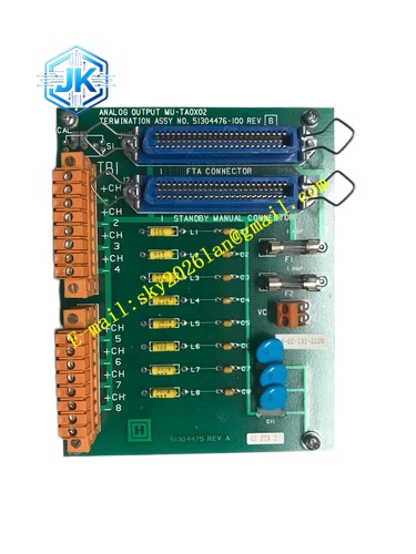
Description
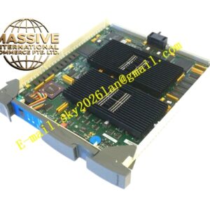
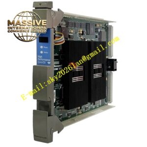
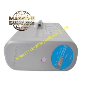
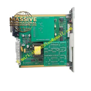
Honeywell 51200523-106
Technical Specifications LCN Bus Rate: 5Mbps Bus Medium: 50Ω coaxial cable Interface Connector: 50Ω BNC connector Logic Power Supply: 5V DC Power Consumption: 6.6W Operating Temperature Range: 0℃ to 65℃ Storage Temperature Range: -40℃ to 85℃ Isolation Withstand Voltage: 1500V AC Relative Humidity: 5% to 95%, non-condensing
Functional Features It executes Manchester encoding for outgoing data frames and decoding for incoming bus signals. It implements CRC check for all transmitted and received data frames. It supports frame retransmission mechanism when frame check error occurs. It continuously monitors bus signal attenuation and frame error rate. It stores communication fault log and network statistical data in non-volatile memory. It uploads link fault and high frame error alarm to LCN network diagnostic console. It receives and forwards system time synchronization frame from LCN master clock.
Application Scenarios LCN network connection for GUS operator stations and HM history modules. Network interface for NIM gateway modules connecting LCN and UCN subnets. Replacement and spare stocking for aging LCN interface boards of legacy TPS cabinets. Communication physical layer support for multi-node LCN network in petrochemical control systems.
Performance Parameters Signal Receiving Sensitivity: 10mV peak Message Encoding/Decoding Latency: ≤60μs Frame Error Log Storage Capacity: 2500 communication fault records Maximum Supported Bus Distance: 2000 meters for LCN trunk cable
Material Composition PCB Substrate: Low-loss high-frequency controlled impedance FR-4 multi-layer board Dual-channel codec FPGA chip RF bus signal transceiver and impedance matching components Gold-plated BNC coaxial connectors Gold-plated back edge fingers Aluminum alloy front panel with anodized anti-oxidation treatment Independent metal shielding cover for RF signal area
Structural Features Standard European pluggable card structure, installed in dedicated LCN node slot of LCN rack. Front panel is equipped with run indicator light, bus link indicator light and fault indicator light. Two groups of BNC connectors are arranged on the side panel for redundant LCN A/B bus wiring. RF signal area is covered by independent metal shielding cover to isolate digital logic noise. High-speed transceiver chips are equipped with dedicated heat dissipation channels to stabilize working temperature.
Working Principle When transmitting data, the board receives parallel data frame from local node processor via backplane bus. The FPGA chip executes Manchester encoding and converts digital data into analog RF signal, then sends signal to LCN coaxial bus through BNC connector. When receiving data, the RF transceiver circuit captures analog signal from bus, completes signal amplification and conditioning, then decodes analog signal into digital frame. The circuit executes CRC verification, sends valid data to local processor and discards error frame. It records frame error count and signal attenuation value, and uploads alarm when communication quality exceeds threshold.
Installation Requirements Insert the board vertically into the dedicated LCN node slot of LCN rack and tighten fixing screws. Use 50Ω dedicated RF coaxial cables for LCN A/B bus wiring. Install 50Ω terminal resistors at the physical ends of LCN trunk buses. Redundant A/B cables shall be laid in separate cable trays to avoid cross interference. After power-on, check link status and error count on the LCN network diagnostic page.
Precautions Release static electricity before plugging the board to protect RF transceiver and FPGA chips. BNC connector oxidation and cable extrusion lead to signal attenuation and intermittent communication dropout. Do not bend coaxial cable with radius smaller than specification limit. Improper terminal resistor installation causes bus reflection and massive frame error. Redundant LCN bus configuration requires two identical interface boards for bumpless switchover.