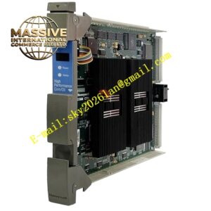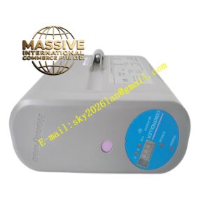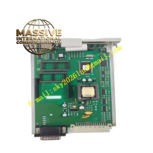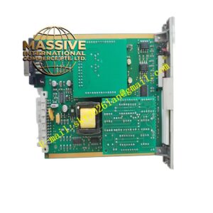



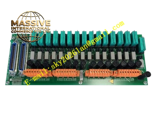
Description
Honeywell 51204166-125
Technical Specifications
- Bus Type: Proprietary parallel DCS backplane bus
- Supported I/O Slot Count: Fixed rack slot allocation
- Distributed Power Rails: +5 V, +12 V, -12 V
- Operating Temperature: 0 °C to +60 °C
- Signal Isolation: LC filter network for power rail noise suppression
- Board Mounting: Rear rack chassis fixed PCB assembly
Functional Features Bus buffer IC regenerates address and data signals to extend bus drive capability across all I/O slots. Impedance matching network suppresses high speed bus signal reflection. Individual slot current limiting circuit isolates shorted I/O slot from entire rack bus and power rail. Power rail LC filter attenuates switching noise generated by plug-in I/O modules. Parity signal routing circuit forwards bus parity error signal back to controller fault register.
Application Scenarios DCS rack rear backplane communication failure spare replacement Intermittent I/O module offline fault repair Preventative spare for old process control DCS overhaul Rack bus signal integrity optimization
Performance Parameters
- Power ripple attenuation: 40 dB minimum at switching noise frequency
- Short circuit isolation response speed: <1 µs
- Parity error capture resolution: Single bus cycle
- Bus signal timing matched to original rack specification
Material Composition Multilayer FR4 PCB, bus buffer logic IC, precision metal film termination resistors, ferrite beads, electrolytic and ceramic decoupling capacitors, pin header connectors for each I/O slot, gold plated edge connector for controller interface.
Structural Features Flat rectangular PCB mounted at rear side of DCS rack chassis. Multiple pin header connectors aligned with each I/O slot backplane pin assignment. Edge connector for mating with main controller board. No front panel, concealed fully inside rack rear assembly. Metal chassis mounting holes for protective earth connection.
Working Principle Controller bus signals enter this board through edge connector. Buffer chips regenerate signal amplitude and driving capacity. Termination resistor network matches parallel bus trace characteristic impedance. Power rails pass through LC filter network before distributing to each slot header. When one slot draws abnormal overcurrent, dedicated limit circuit cuts off that slot power and bus signal path without affecting remaining rack slots.
Installation Requirements Rack must be fully de-energized before removing or installing this board. Align all pin headers carefully to avoid bent pins. Secure mounting screws to rack metal chassis to establish reliable protective ground. Run controller system diagnostic test after replacement to verify all I/O slots communication.
Usage Notes Do not remove or replace termination and filter components on board. Handle board with anti-static protection at all times. Bent pin headers cause intermittent I/O communication faults. Keep rear rack area clean from conductive dust accumulation.