


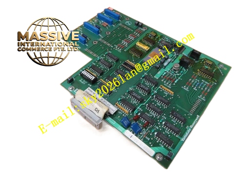
Description
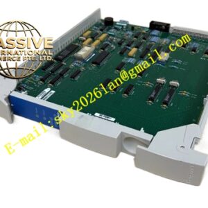
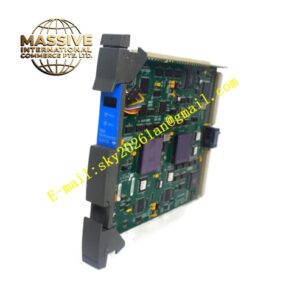
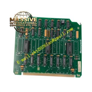
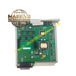
Honeywell 82408512
Technical Specifications
- Compatible slot: HPM main processor board dedicated daughter slot
- I/O Link channel count: 4 independent bus channels
- Maximum connected I/O modules per channel: 16
- Communication rate: 1 Mbps
- Onboard buffer memory: 128 KB
- Supply power: 5 V DC from HPM main board
- Operating temperature: 0 °C to +60 °C
- Hot swap support: Online replacement for faulty daughter boards
Functional Features Independent FPGA logic controls I/O bus communication, does not consume main processor compute resources. 4-channel parallel scanning drastically reduces total I/O acquisition cycle time. Per-channel bus CRC communication verification, ultra-low data transmission error rate. Automatic bus fault diagnosis, identifies channel disconnection and module communication failure. Per-channel LED status indicator, provides visible bus health status for maintenance. On-board bus termination resistors, eliminates long-distance communication signal reflection.
Application Scenarios Field I/O point expansion for HPM process managers Spare part replacement for HPM bus communication faults in legacy systems I/O interface assembly for new chemical plant HPM installations Expansion retrofits for existing process control I/O capacity
Performance Parameters
- Single-channel scan cycle: 5 ms
- Communication latency: ≤1 ms
- Fault detection response: ≤100 ms
- Data buffer hit rate: ≥99%
- Maximum bus transmission distance: 30 meters shielded twisted pair
Material Composition FR4 high-speed PCB substrate FPGA communication processing chip High-speed SRAM buffer chip Gold-plated board-to-board connector Optocoupler isolation devices TVS surge protection diodes
Structural Features Small rectangular PCB daughter board. Rear gold fingers plug directly into the HPM main processor board slot. Front flat cable connectors interface to field I/O subracks. Channel silk-screen labels printed next to each connector. Impedance-controlled trace layout matches I/O bus 120 Ω characteristic impedance.
Working Principle After power-up, the board FPGA initializes I/O Link communication logic, polling connected field I/O modules across 4 bus channels in fixed order. Output commands from the main processor are sent to corresponding I/O modules via the bus; collected field input data returns to the board buffer. The main processor reads buffered data as needed for logic computation. Bus monitoring circuits continuously check communication signal integrity, generating channel fault flags to the main CPU when communication is lost. Termination resistors absorb signal reflection at the bus end, ensuring reliable long-distance communication.
Installation Requirements Insert the daughter board into the dedicated slot only when power is off, press evenly until gold fingers are fully seated. Connect I/O bus flat cables to matching channel positions, lock the connector clips to prevent loosening. Check LED status after power-up, confirm all connected I/O modules are detected by the main processor. Wear an anti-static wrist strap when handling the board to avoid ESD damage to the FPGA.
Usage Notes Hot-swapping the daughter board causes all connected I/O channels to drop offline, triggering process alarms. Oxidized connector contacts cause channel dropouts; clean gold contacts regularly. Daughter board firmware version must match the HPM main processor firmware; mismatched versions prevent board recognition. Never short on-board termination resistors, this causes bus signal reflection and communication failure.