


Description
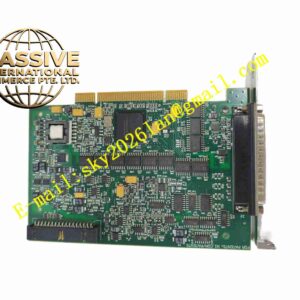
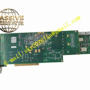
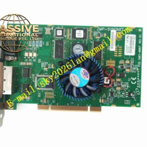
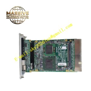
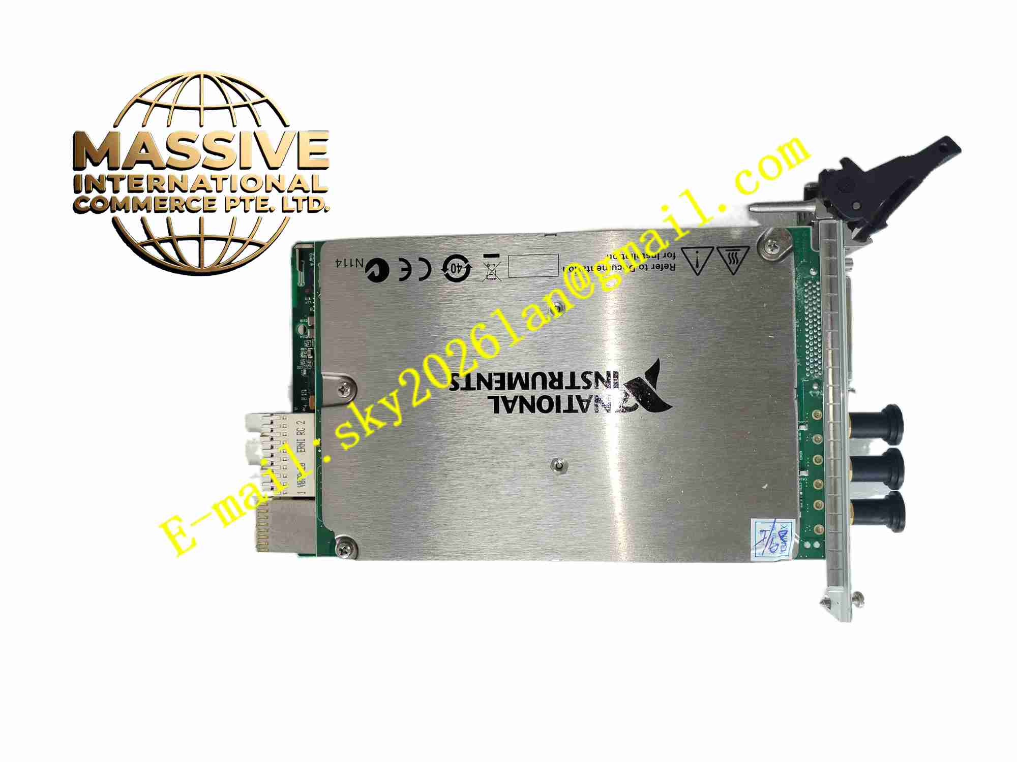
NI PXIe-6544 Digital I/O Module
Technical Specifications Model: PXIe-6544 Form Factor: 3U single slot PXI Express module Digital Channel Count: Multiple bidirectional digital I/O channels Logic Voltage Level: Configurable digital logic voltage Maximum Data Rate: High-speed parallel pattern rate Front Connector: High density digital signal connector Operating Temperature: 0 ℃ ~ +55 ℃ Storage Temperature: -40 ℃ ~ +70 ℃ Relative Humidity: 10% ~ 70% non-condensing Onboard Memory: Dedicated pattern memory for waveform storage Synchronization: PXI trigger bus and star trigger support
Functional Features Bidirectional digital channels can be configured as digital pattern output or digital input acquisition. Large onboard memory stores test pattern sequence to realize burst high-speed pattern playback. Programmable digital logic voltage to match different DUT logic families. Hardware trigger function starts pattern generation or capture according to external trigger signal. PXI trigger bus synchronizes digital test sequence with analog measurement instruments. Per-channel overvoltage protection prevents damage from external abnormal voltage. Compatible with NI-HSDIO instrument driver for digital pattern programming. Supports pattern looping and conditional branch execution in hardware sequence engine.
Application Scenarios Digital integrated circuit functional test, FPGA verification test, memory chip test, digital communication interface test, automotive digital circuit validation, automated semiconductor production test.
Performance Parameters Maintain specified data rate and signal integrity under rated operating temperature. Hardware pattern engine executes pre-stored pattern sequence with precise timing control. Per-channel protection circuit limits overvoltage to protect module internal circuit. Trigger circuit realizes low latency synchronization with other PXIe instruments. Onboard memory supports continuous pattern playback without host streaming bottleneck. Signal output timing jitter keeps within specified tolerance range.
Material Composition Module Housing: Flame-retardant plastic front panel and metal shielding frame. Main PCB: FR4 multi-layer high-speed digital printed circuit board with conformal coating. Core Electronic Components: FPGA, high-speed I/O buffer chips, pattern memory chips, level translation chips, static protection array, power monitoring IC. Connector: Gold-plated high-density front signal connector and gold-plated PXIe backplane edge connector. Indicator Components: LED status indicators on front panel. Fasteners: Stainless steel screws and metal shielding clips.
Structural Features 3U single-slot standard PXIe module mechanical dimension. Front panel carries high-density digital signal connector and LED status indicators. Metal shielding shell suppresses high-speed digital signal electromagnetic radiation. Rear gold-plated edge connector mates with PXIe chassis backplane for power and PXIe bus communication. Internal circuit separates high-speed digital I/O front-end circuit and FPGA control circuit. Ventilation gaps reserved for chassis forced cooling airflow.
Working Principle PXIe chassis backplane provides DC power and PXIe bus communication signal to PXIe-6544 module. Host PC downloads digital test pattern and timing parameters into onboard memory of module through PXIe bus. Onboard FPGA controls high-speed I/O buffer to output digital pattern sequence according to preset timing. When module is set to input acquisition mode, FPGA captures digital signal state from DUT and stores sampled data into onboard memory. Hardware trigger circuit monitors trigger signal from PXI trigger bus or external input, and starts or stops pattern sequence execution once trigger condition meets. Level translation circuit converts internal logic level to user-configurable DUT logic voltage. Overvoltage protection circuit limits abnormal voltage on each channel to protect internal chips. Captured digital data is uploaded to host controller via PXIe bus after test completion.
Installation Requirements Power off PXIe chassis before inserting or removing module. Align module with empty PXIe slot, push steadily until backplane connector fully engages and front panel locks. Connect DUT digital test cable to front high-density connector. Install NI-HSDIO instrument driver and NI MAX configuration software on host computer. Power on chassis, complete hardware identification and channel parameter configuration. Set logic voltage, pattern sequence and trigger parameters in test software. Reserve cooling airflow space around module slot.
Usage Precautions Do not apply voltage exceeding configured logic voltage range to digital channels. Use matched high-speed shielded test cable for digital signal wiring, control cable length to reduce signal reflection. Separate high-speed digital signal cables from analog measurement cables. Prevent condensation and conductive dust inside PXI chassis. Do not disassemble module shielding housing without professional authorization, static sensitive components exist on PCB. Check test cable contact integrity regularly in long-term test system. Carry out periodic calibration according to manufacturer specification.