


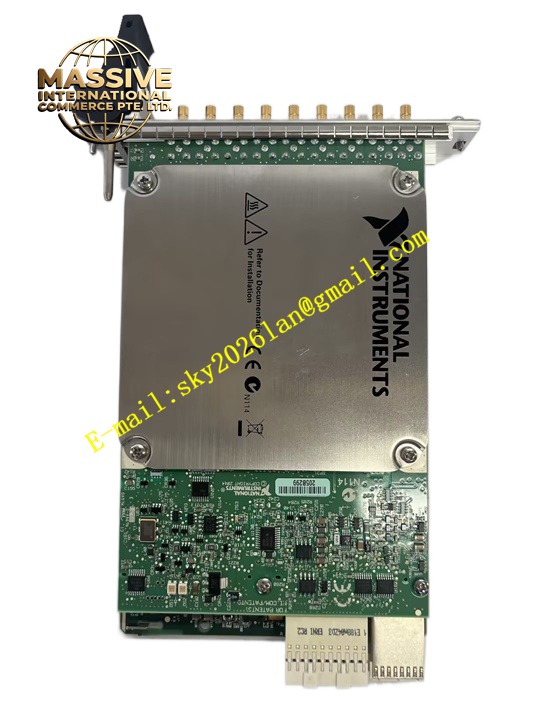
Description
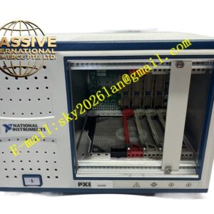
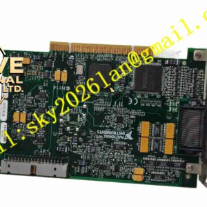
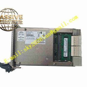
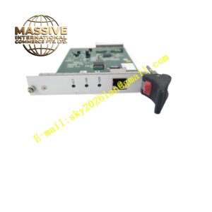
NI PXIe-5105 Oscilloscope Module
Technical Specifications Model: PXIe-5105 Form Factor: 3U single slot PXI Express module Channel Count: 8 analog input channels ADC Resolution: 12-bit Maximum Sampling Rate: 60 MS/s per channel Input Bandwidth: 60 MHz Input Coupling: AC or DC coupling configurable Input Impedance: 1 MΩ Front Connector: 37-pin D-SUB connector Operating Temperature: 0 ℃ ~ +55 ℃ Storage Temperature: -40 ℃ ~ +70 ℃ Relative Humidity: 10% ~ 70% non-condensing
Functional Features 8 independent analog input channels for multi-channel waveform synchronous acquisition. 12-bit high speed ADC captures fast transient voltage signals. Configurable AC/DC input coupling and programmable voltage input range. Multiple trigger modes including edge trigger, window trigger and software trigger. Onboard memory for waveform data buffering to avoid data loss during high-speed capture. PXI trigger bus realizes synchronous acquisition with other PXIe instruments. Compatible with NI-SCOPE instrument driver for waveform programming and analysis. Built-in overvoltage protection on each input channel.
Application Scenarios Power supply transient waveform test, digital circuit signal integrity measurement, sensor pulse signal capture, automotive electronic transient test, relay switching characteristic test, automated production line waveform inspection.
Performance Parameters Maintain specified bandwidth and sampling accuracy under rated operating temperature. Overvoltage protection circuit activates when input voltage exceeds maximum rated range. Multi-channel synchronous sampling keeps consistent time base between all channels. Onboard buffer memory stores waveform data during burst sampling. Input circuit maintains stable impedance characteristic within full bandwidth. Trigger circuit can capture low amplitude transient pulse signal reliably.
Material Composition Module Housing: Flame-retardant plastic front panel and metal electromagnetic shielding frame. Main PCB: FR4 multi-layer high-speed printed circuit board with conformal protective coating. Core Electronic Components: 12-bit high-speed ADC chips, analog front-end amplifier, input protection circuit, FPGA, high-speed memory chip, reference voltage chip. Connector: Gold-plated 37-pin D-SUB front connector and gold-plated PXIe backplane edge connector. Indicator Components: LED status indicators on front panel. Fasteners: Stainless steel screws and metal shielding brackets.
Structural Features 3U single-slot PXIe standard module mechanical structure. Front panel with 37-pin D-SUB signal connector and module status LED indicators. Integrated metal shielding structure suppresses high frequency electromagnetic interference. Rear gold-plated edge connector connects to PXIe chassis backplane for power and high-speed PXIe bus transmission. Internal circuit layout separates high-speed analog front-end circuit and digital FPGA circuit. Ventilation openings for forced air cooling from chassis fan.
Working Principle PXIe chassis backplane supplies DC power and PXIe high-speed communication signal to PXIe-5105 module. Analog input signal enters module through 37-pin D-SUB connector. Signal passes through programmable attenuation circuit, AC/DC coupling circuit and input overvoltage protection circuit. The conditioned analog signal is sent to 12-bit high-speed ADC to convert analog waveform to digital sampling points. Onboard FPGA controls sampling timing, trigger judgment and waveform data storage into onboard buffer memory. When trigger condition is met, FPGA reads waveform data and transmits data stream to host computer through PXIe bus. Host software reconstructs waveform and completes measurement and analysis.
Installation Requirements Cut off PXIe chassis power before installing or removing module. Insert module into empty PXIe slot, push steadily until backplane connector fully engages and front panel locks. Connect test signal probes to front D-SUB connector according to channel definition. Install NI-SCOPE instrument driver and NI MAX configuration software on host PC. Power on chassis, complete hardware identification and channel parameter configuration. Set input range, coupling mode, sampling rate and trigger parameters in software. Reserve cooling airflow space around module slot.
Usage Precautions Do not apply input voltage exceeding maximum rated input range to channels. Use 50Ω or 1MΩ matched high-frequency shielded coaxial cable for high-speed signal measurement. Keep signal cable away from high-power switching cables to reduce noise coupling. Do not operate in environment with condensation, corrosive gas or conductive dust. Do not disassemble shielding housing without professional authorization, high-speed circuit is sensitive to static discharge. Check cable shielding integrity regularly for long-term continuous test system. Execute periodic calibration according to manufacturer requirements.